WAFER INSPECTION & METROLOGY
Enhancing the most advanced wafer processing systems.
We offer solutions for thin film measurement, optical wafer inspection, electron beam inspection, microscopy and reticle/mask inspection.
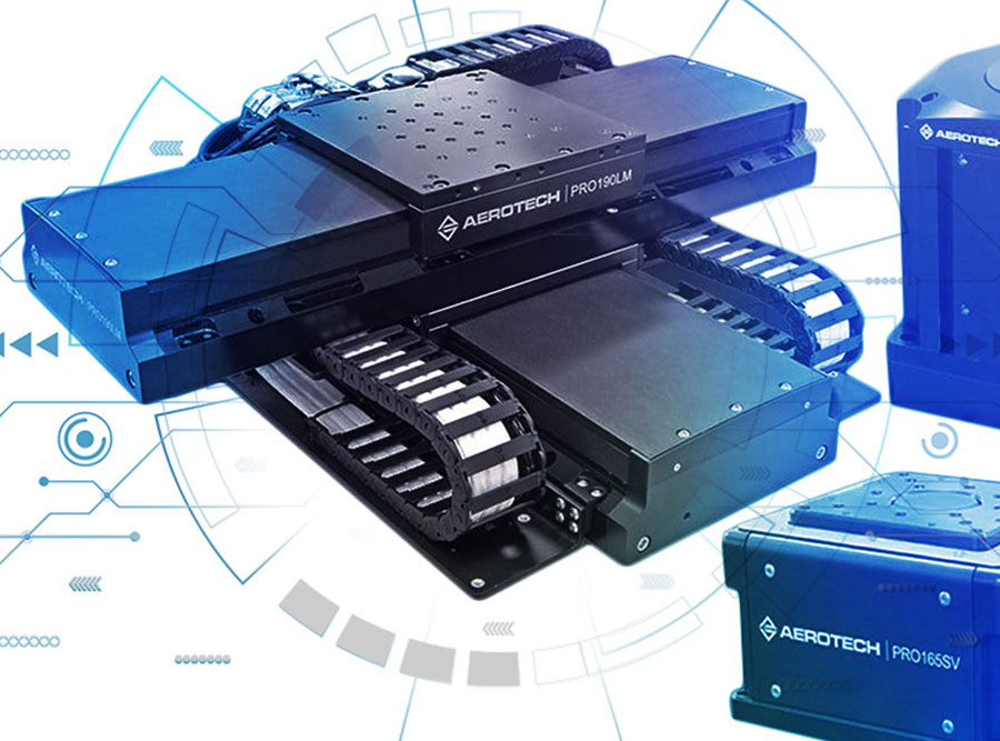
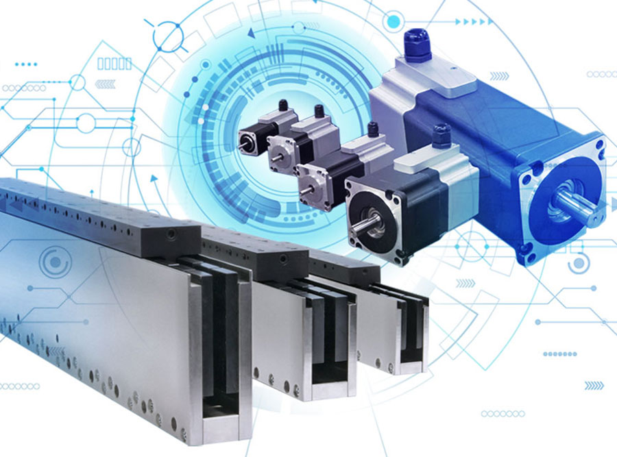
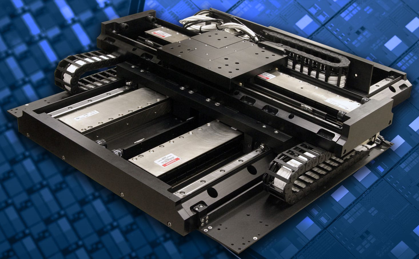
The Most Versatile Positioning Solutions
We have 50+ years of experience designing standard serial-stacked wafer stages, low-profile integrated XY stages and planar air-bearing solutions for the wafer inspection market. When a standard system doesn’t work, we can build a custom solution for your exact needs.
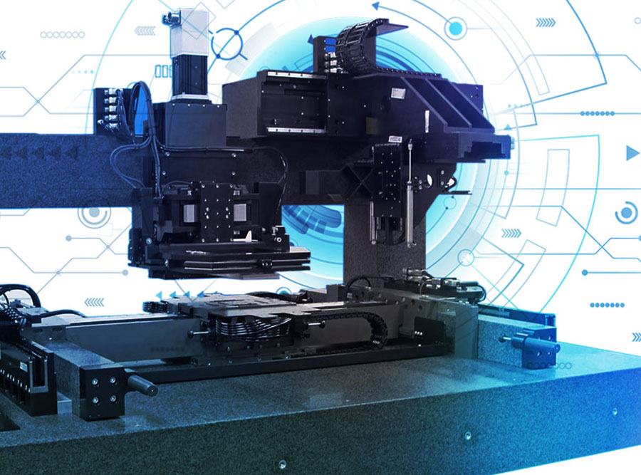
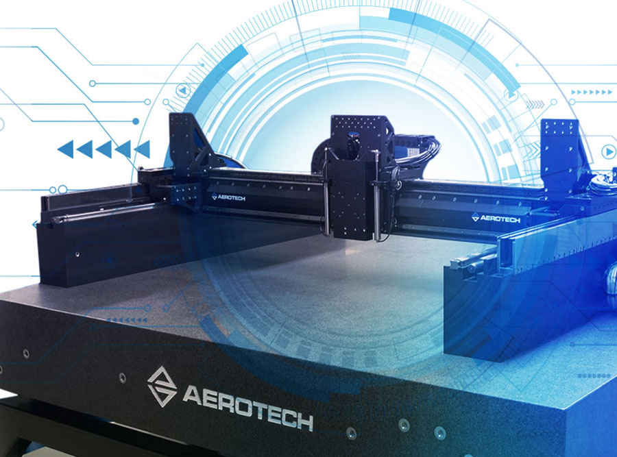
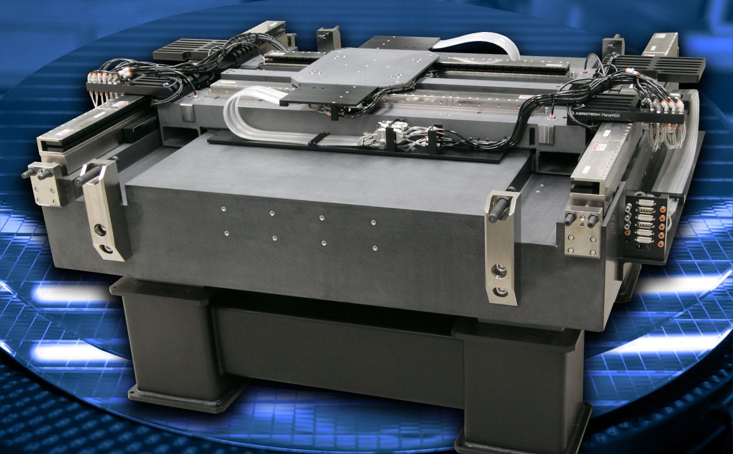
The Ultimate in Precision
Our planar air-bearing solutions, coupled with laser interferometry, minimize wafer-plane errors and Abbe offset. Advanced silicon carbide solutions with advanced controls deliver nanometer-level positioning with high wafer-per-hour throughput.
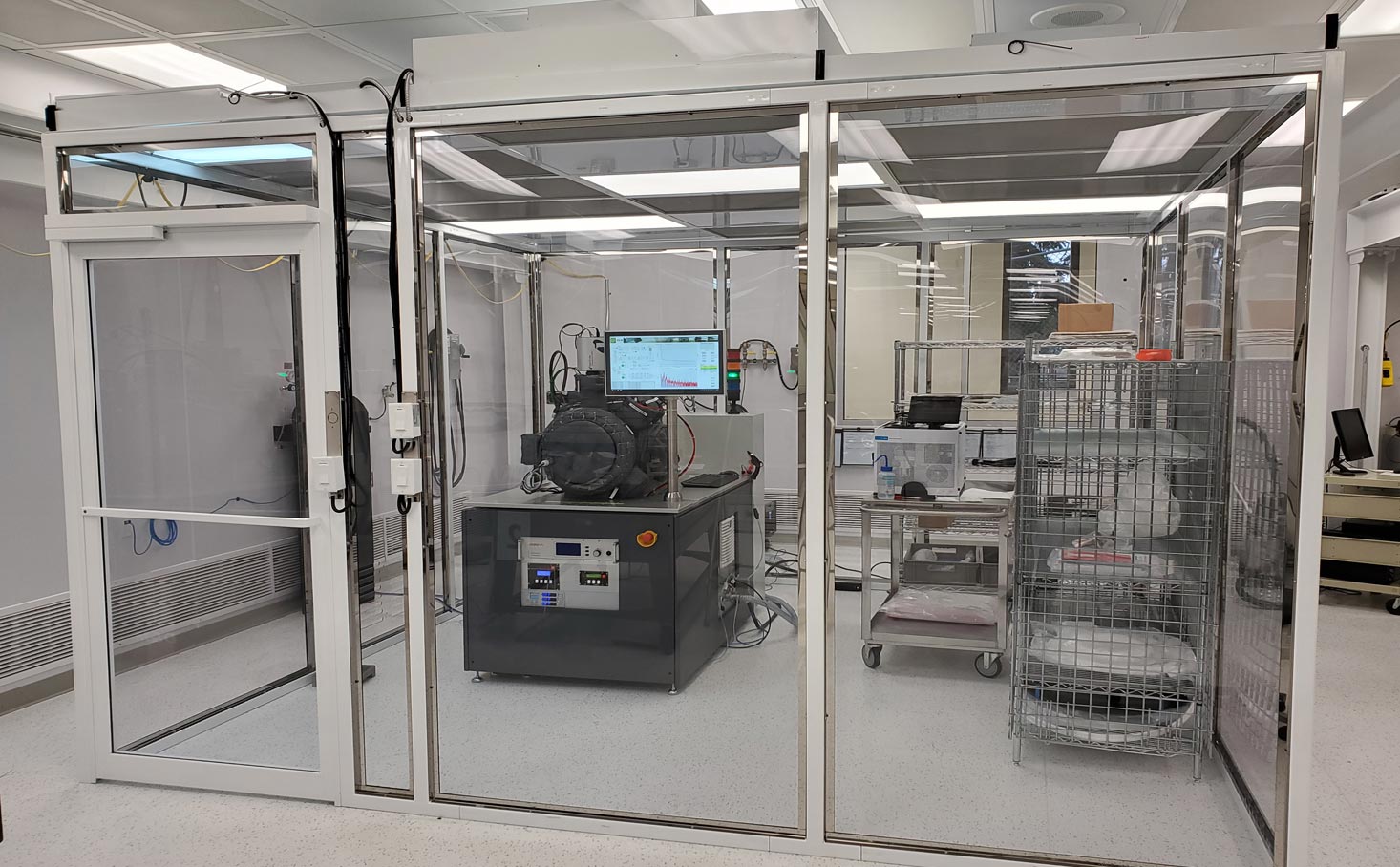
Cleanroom Manufacturing
We operate with the highest levels of cleanliness for next-generation wafer processing. Our temperature-controlled, ISO Class 6 cleanroom facilities with cell-specific ISO Class 5 capability ensure the high-quality, reliable manufacturing of our positioning solutions.